CMOS VLSI Design The rules describe the minimum width to avoid breaks in a line minimum spacing to avoid shorts between lines and minimum overlap to ensure that two layers completely overlap. List of Rules to be Considered 7.
Vlsi Design Cmos Layout Ppt Download
If contact is needed show explicitly.
. CMOS VLSI Design Digital Design Overview Physical principles Combinational logic Sequential logic Datapath Memories Trends Dopants Silicon is a semiconductor Pure silicon has no free carriers and conducts poorly Adding dopants increases the conductivity Group V. CMOS λ Design Rules. When two or more sticks of different type cross or touch other there is no electrical contact.
NWELL Width Space 13. Winner of the Standing Ovation Award for Best PowerPoint Templates from Presentations Magazine. VLSI DESIGN Course Coordinator.
Theyll give your presentations a professional memorable appearance - the kind of sophisticated look that. Rules for Drawing Stick Diagrams. Layout Design Rules 2 Introduction Layout Rules Is Also Referred As Design Rules It Is Considered As A Prescription For Preparing Photomasks Ppt Download Vlsi Design Cmos Layout Ppt Download.
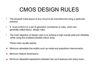
Design Rules Allow for a ready translation of a circuit concept into an actual geometry in silicon Provide a set of guidelines for constructing the. Missing electron called hole p-type nMOS Operation Body is commonly tied. Each of the rule numbers may have different values for different manufacturers.
How to build a good CMOS chip 0. VLSI Design Lecture PPTs INSTITUTE OF AERONAUTICAL ENGINEERING Dundigal Hyderabad -500 043 632015 1 Department. 57035 Course Title.
I They guarantee that the transfers onto the wafer preserve the topology and geometry of the patterns. CMOS Formation - P diffusion 5. Rabaey Cross-Section of CMOS Technology Design Rules Interface between designer and process engineer Guidelines for constructing process masks Unit dimension.
Introduction to CMOS VLSI Design Circuits Layout Outline CMOS Gate Design Pass Transistors CMOS Latches Flip-Flops Standard Cell Layouts Stick Diagrams CMOS Gate Design Activity. Theyll give your presentations a professional memorable appearance - the kind of sophisticated look that. Susanta Sen Institute of Radio Physics Electronics University of Calcutta.
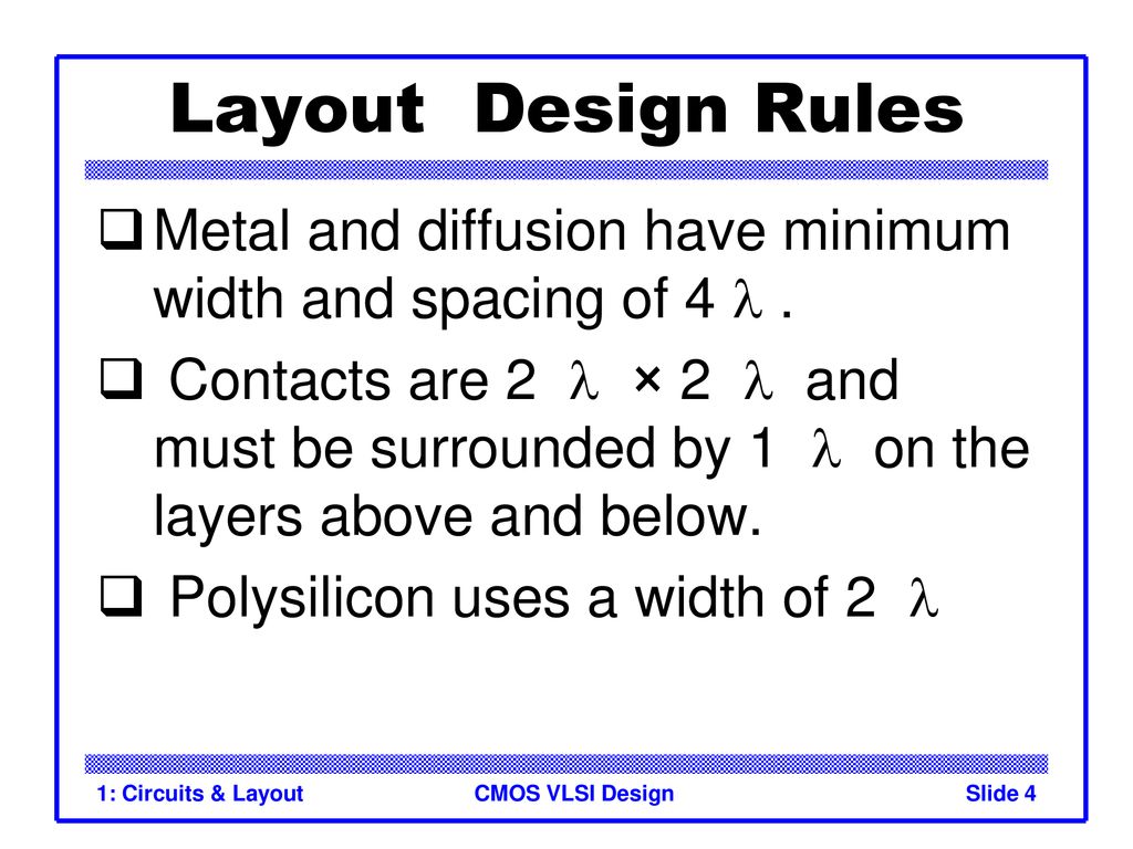
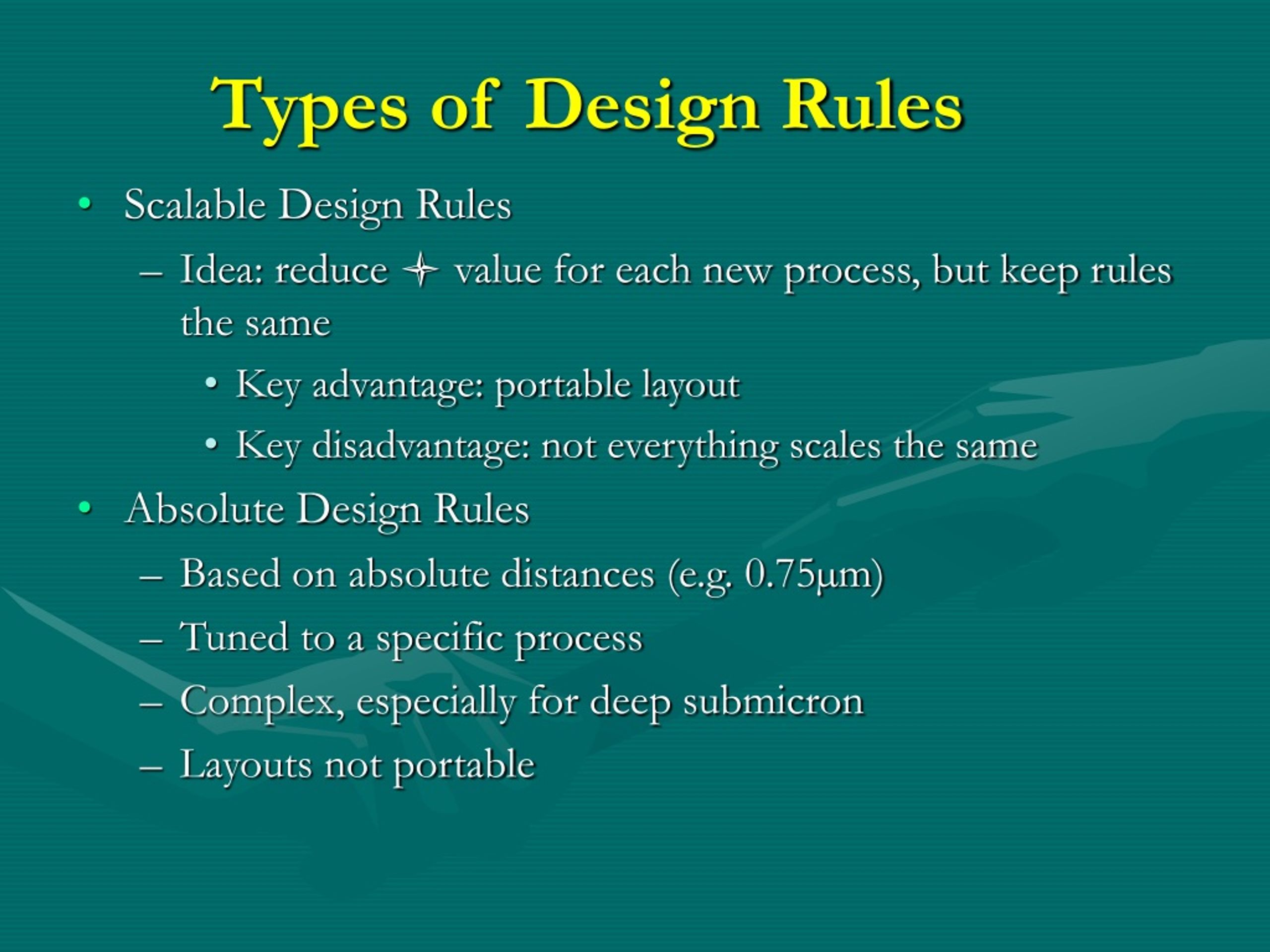
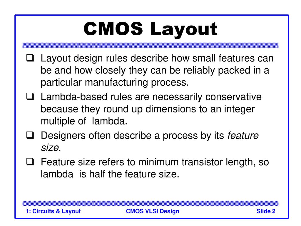
VLSI Systems Design Design Rules for CMOS Lecture 7. Lambda Based Design Rules Design rules based on single parameter λ Simple for the designer Wide acceptance Provide feature size independent way of setting out mask Minimum feature size is defined as 2 λ Used to preserve topological features on a chip Prevents shorting opens contacts from slipping out of area to be contacted. Low power vlsi design ppt Apr.
Transistor Layout Two rectangles 1. Sketch a 4-input CMOS NOR gate Complementary CMOS Complementary CMOS logic gates nMOS pull-down network pMOS pull. Lambda parameter absolute dimensions micron rules CMOS Process Layers Intra-Layer Design Rules Transistor Layout Vias and Contacts Select.
University of Puerto Rico at Mayagüez. Rule 31 for example is the minimum width of poly 2 l. Lambda λ-based design rules Author.
Sheshagiri Rao Professor Team of Instructors B. Low power vlsi design ppt 100 Share. Metal-Oxide-Semiconductor Field-Effect Transistor N-type MOS NMOS and P-type MOS PMOS Voltage-controlled switches A MOSFET has four terminals.
Introduction Silicon Lattice Transistors are built on a silicon substrate Silicon. Kiran Kumar Assistant Professor Course Structure. When two or more sticks of the same type cross or touch other that represents electrical contact.
Minimum separations minimum and maximum widths overlap rules I Scalable rules. Interconnect Transistors Place metals and vias Spec2Layout2 2. This Presentation slides consists of the various design rules associated with layout stick Diagrams with basic CMOS Gates explained.
26 2014 100 likes 103548 views Download Now Download. CMOS Layout Example 6. Winner of the Standing Ovation Award for Best PowerPoint Templates from Presentations Magazine.
Worlds Best PowerPoint Templates - CrystalGraphics offers more PowerPoint templates than anyone else in the world with over 4 million to choose from. Layout and Cross Section - NMOS 8. Design rules I The geometric design rules are a contract between the foundry and the designer.
23 CMOS Design Rules. The MOSIS stands for MOS Implementation Service is the IC fabrication service available to universities for layout simulation and test the completed designs. Complementary Metal Oxide Semiconductor Fast cheap low power transistors Today.
In a 06 µm process this corresponds to an actual width of 12 µm and a length of 06 µm. Minimum line width scalable design rules. How to build your own simple CMOS chip CMOS transistors Building logic gates from transistors Transistor layout and fabrication Rest of the course.
Extra electron n-type Group III. Circuits Layout CMOS VLSI Design Slide 45 Gate Layout qLayout can be very time consuming Design gates to fit together nicely Build a library of standard cells qStandard cell design methodology V DD and GND should abut standard height Adjacent gates should satisfy design rules nMOS at bottom and pMOS at top. The MOSIS rules are scalable λ rules.
Layout Design Rules - Free download as Powerpoint Presentation ppt pptx PDF File pdf Text File txt or view presentation slides online. Electrical and Computer Engineering Department. Transistor dimensions are often specified by their WidthLength WL ratio.
To direct and control logic signals in IC design MOSFET. Sketch a 4-input CMOS NAND gate CMOS Gate Design Activity. Spec2Layout2 CMOS Logic Circuits made of Transistors only Design transistors Place Gate electrode Poly-Si Cross over the diffusion window.
ELECTRONICS AND COMMUNICATION ENGINEERING Course Code. SlideShare uses cookies to improve functionality and performance and to provide you with relevant advertising. Gate source drain and substrate body Complementary MOS CMOS Using two types of MOSFETs to create logic networks NMOS PMOS.
Worlds Best PowerPoint Templates - CrystalGraphics offers more PowerPoint templates than anyone else in the world with over 4 million to choose from. Design Rules Jan M. Figure 211 defines the design rules for a CMOS process using pictures.
CMOS lambda Design Rules. Arrows between objects denote a minimum spacing and arrows showing the size of an object denote a minimum width. Lambda Based Rules 9.
The MOSIS design rules are as follows. 1 Rules for N-well as shown in Figure below. I These rules are the designers interface to the fabrication process.
Cmos Design Rule

Cmos Design Rule

Cmos Design Rule

Ipv4 Header Packet Switching Ipv4 App Design
Vlsi Design Cmos Layout Ppt Download

Introduction To Cmos Vlsi Design Lecture 1 Circuits Layout Lecture Design Rules Dry Erase Markers
Ppt Layout Design Rules Powerpoint Presentation Free Download Id 9170183

Inverter Design In Cadence Design Rules Design Mechanical Engineering
0 comments
Post a Comment